


The choice of mounting orientation, termination styles, pad dimensions and sizes used for surface mount passive resistive components are some of the factors that contribute to the device’s performance in an RF circuit layout. Determining the trade off between these factors in addition to ease of component-to-PCB assembly, solderability, ruggedness and other design optimization for power and RF performance could be an onerous task for RF engineers. The purpose of this technical note is to shine light on the advantages and/or disadvantages of these mounting techniques and termination styles in high frequency applications.
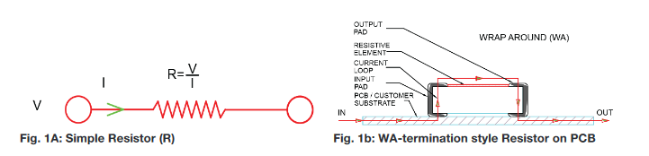
Fig. 1A & 1B above are simple illustrations of an SMT resistor wraparound termination style. At DC, the resistor is simply governed by ohm’s law’s Current, Resistance and Voltage relationship (R=V/I) whose impedance Z is simply equal to R. However in an RF environment, certain parasitic effects and contributions must be understood and accounted for as shown in Fig 2 below. The equivalent circuit diagram of Fig 2 below is a more appropriate representation of the simple resistor described above.
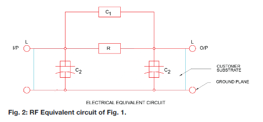
From the equivalent circuit, C1 is the shunt capacitor that is formed between the input and output pads of the full wraparound termination style device. This capacitor is in series with the application’s circuit PCB layout but in parallel with the resistive element. It is known that capacitance C is related to the surface area of the plates that 1 formed it (equation 1 below), the distance d between plates and the substrate material properties.
C= (A * r)/D ………………………………eq 1, [1]
Where;
A= Surface area of plates, (A= w*t); w is the width (w) and t is the thickness of substrate
D = distance, in this case it’s the length of the part, the distance between each end of the wraparound.
r = the dielectric constant of substrate. Example for alumina, the dielectric constant is 9.5 – 9.8.
(Based on the grade of alumina substrate)
This capacitor is directly under the resistive film element. As frequency increases, the capacitance value, which is in parallel with the DC resistance eventually becomes the dominant high frequency impedance. The higher the DC resistor value, the more the capacitive effect becomes dominantly prevalent. In other words, a low ohmic value resistor will have less of a capacitive effect than a large ohmic value resistor since the same capacitance will act to change both resistor values. For example, if a 5K ohm, 5% WA (Wraparound) resistor with 1pF parasitic capacitor is installed in an RF 1GHz application, the parasitic capacitance will present a reactance XC that is in parallel with the DC resistance as given in the equation 2 below;
XC = 1/(2π f C) Ω …………..eq 2
Where,
XC = Capacitive-Parasitic Reactance (ohm)
F= Frequency (Hz)
C= Capacitance (Farad)
If we consider three scenarios relating to the above example as follows;
Case 1: In this example, XC is calculated to be = 159Ω, i.e. XC = 1/(2*6.28*1pF*1GHz) and since this is in parallel with the DC resistance, the effective resistance is 5KΩ//159Ω = 154Ω. This 154Ω is the effective resistance (Impedance-Z) at 1GHz as opposed to the 5000Ω that was originally intended. This significant disparity between the two values is one of the pitfalls to be recognized by the RF engineer.
Case 2: Assuming the capacitance value was smaller in the example above, the magnitude of the difference between the DC resistance and the effective resistance would be less pronounced since XC would increase relative to the DC resistance. For instance, if the capacitance was to be 0.1 pF as opposed to 1pF, XC would be 1591.54Ω, about 10 times larger, and the final effective impedance would be 5000//1591.54 = 1207Ω. While this value is still not a matched impedance value, it’s a lot closer than 154Ω. On the other hand if the frequency is increased to 10GHz, (10 times the original frequency at 1pF), the reactance is also reduced by about 10 times (15.9Ω), such that the 5kΩ resistor is now effectively measuring just under 16Ω, a huge difference.
Case 3: Assuming that the nominal resistance was only 50Ω, and the capacitance was 0.1pF, then the impedance (Z) would compute to 50Ω//1591.54 = 48.47Ω, still within the 5% tolerance. Thus there would be no noticeable parasitic issue. In general, a bad combination is found when the resistor value is high and parasitic capacitance is high.
The capacitor C2 from Fig. 2 above displays the parasitic effects which occur only when the device is installed on a customer’s substrate or PCB. This parasitic can be capacitive or inductive depending on the application’s line width. If the customer line width is much narrower than the part, the DUT will look like a parallel capacitor. In order to determine this capacitance the feed line sizes must be known; i.e. the relation of the part to the feed lines determines the capacitance value. Similarly, most of the inductive parasitic effects happen only when the device is installed into the customer’s substrate. From the Fig. 2 above the value of the inductance L1 is dependent largely on the size of the customer’s feed lines. If the customer line width is much wider than the SMT (DUT) part, the part will look like a series inductance.
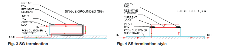
Other termination styles like the SS (single sided with no wrap-Fig. 4) or the SG (single wrap to ground plane-Fig. 3) and the partial wrap (PW-Fig. 5) termination styles all have better parasitic performance than the WA style described above under similar layout and operating conditions. The SG termination style and the SS termination style (Fig. 3 & 4) below would not have any series parasitic capacitor between the input and the output pads (C1) making them more RF efficient than WA termination style under similar layout and operating conditions. However, the SG and the SS styles would both still have lead inductances, the magnitudes of which are largely dependent on the mounting techniques employed.
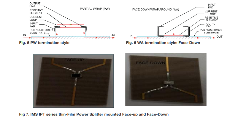
Face-down Mounting: A resistive passive device is considered mounted face-down when the resistive element is facing to the substrate as against the regular face-up orientation. The PW (Partial Wrap) style in Fig. 5 has similar parasitic characteristics to that of the full wrap (WA) except that they are negligibly small and can be neglected when mounted face-down. Face-down mounting also have the advantages of reduced current loop area and lower ESL (Equivalent series inductance). This reduced ESL provides for better resistor stability [2] and good frequency response. The wraparound termination style (WA) in Fig. 1b above is mounted in a conventional SMD face up on a customer’s substrate, the red arrowed line shows a wider current loop area for this mounting technique than a similar part mounted face-down (Fig. 6); the increased loop area for the face-up configuration proportionally increases the magnitude of the parasitic inductance (LA) as shown from the equation 2 below. The equation shows the relation of the inductance L and the current loop area for a solenoid. From this relationship, the reduced current loop area and the resulting smaller series inductance (ESL) of the facedown mounting are the features that contribute to its improved RF performance when compared to the regular face-up mounting of similar part.
L= µN2 Al ……………………..eq 2, [2]
Where; L= Inductance (nH)
µ =Permeability factor
N=Number of turns per unit length
A=Area of current loop
L=length.
Additional advantages of the face-down mounting technique are improved power handling capability and reduced overall insertion loss. For example, The IMS A-Series thin film attenuators are designed for low noise high freq to 10GHZ applications. The A- 0402 size when mounted face-down (IMS2652) with good RF design layout performs efficiently to 40GHZ (0402 size) with excellent VSWR (see Fig. 8 below). Also the newly released IPT thin-film broadband resistive power splitters (Fig. 7) are designed to operate to 20GHZ; the same part when mounted face-down with good RF layout operates to 30GHZ and above (0402 size) with typical VSWR of 1:1.3
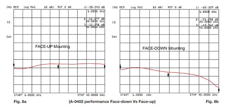
In conclusion, for higher frequency applications (to 40GHZ or higher), the performance benefits and cost saving advantages of face-down mounting are huge since the same component that’s employed for lower frequency applications can also be designed for higher frequency applications without the concern of trading off power handling capability and cost.
For the manufacturing convenience of those customers desiring face-down mounting and for the ease of device assembly, IMS has devised a means for some of these parts to be ordered pre-packaged as face-down orientation on tape and reel. This is especially good for pick-n-place manufacturing environments to prevent assembly mistakes and wrong polarity issues for components with different lead polarities.
For additional info and technical support for high freq applications of passive SMT devices and other IMS products, please contact technical support at techsupport@imsresistors.com
REFERENCES
[1] Losee, A. Ferril, RF Systems, Components and Circuits Handbook, 2nd Edition Artech House 2005 pp346
[2] Prymak, John; Blais, Peter; Long, Bill; Staubli Paul “Improved Ripple Current with Facedown Terminations” CARTS-Europe 2007 Conference
Download a our white paper here.